Photonic Integrated Circuits
Research on Photonic Integrated Circuits (PICs)
The realization of semiconductor-based integrated circuits with specific functionalities is an important field of current ongoing research activities. While initial work in this field historically focused on “electronical devices” like transistors to increase the number of functional units within a given footprint, nowadays optoelectronic devices have moved into the focus of such activities. Besides implementing different functional devices like emitters, detectors, amplifiers or modulators on the chip-scale such small and compact devices allow to efficiently reduce the consumed power of otherwise discrete bulky tabletop setups. This will contribute to the worldwide activities to reduce power consumption in order to limit effects of climate change and global warming. This field of research is therefore often referred to as “green photonics” or energy-efficient photonics. How much the efficiency of such integrated devices can be further improved remains to be seen. However, it can be expected that the overall power consumption of a photonic integrated circuits (PICs) is 1-2 orders of magnitude smaller than of its tabletop counterpart.
Plasmonic integration: sensing vs directing
In previous years the main attention in the field of mid-infrared optoelectronics was given to successfully advance individual discrete components like quantum cascade lasers (QCLs), QC detectors (QCDs) or interband cascade lasers (ICLs). With the increasing level of maturity of those devices, miniaturization and integration became more relevant, to realize small and compact devices for, e.g. sensing applications.
In our group we work on such PICs by using concepts such as monolithic and hybrid integration. They rely on using suitable waveguide concepts that enable coupling and guiding of the light between the individual active components. Based on initial results from literature, which introduced novel dielectric-loaded surface plasmon polariton (DLSPP) waveguides [1], we further exploit and develop this concept into the next generation of monolithic mid-infrared PICs.
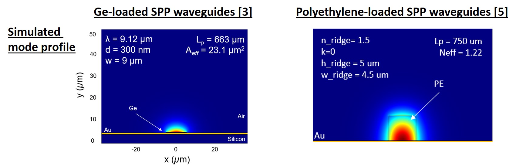
An important characteristic of such plasmonic waveguide is their ability to either be suitably used for sensing applications by guiding the light mainly (> 95%) in the surrounding medium [1-3] or by allowing to guide and direct the light along the chip-surface [4,5]:
a. Mid-infrared PICs for dynamic reaction monitoring
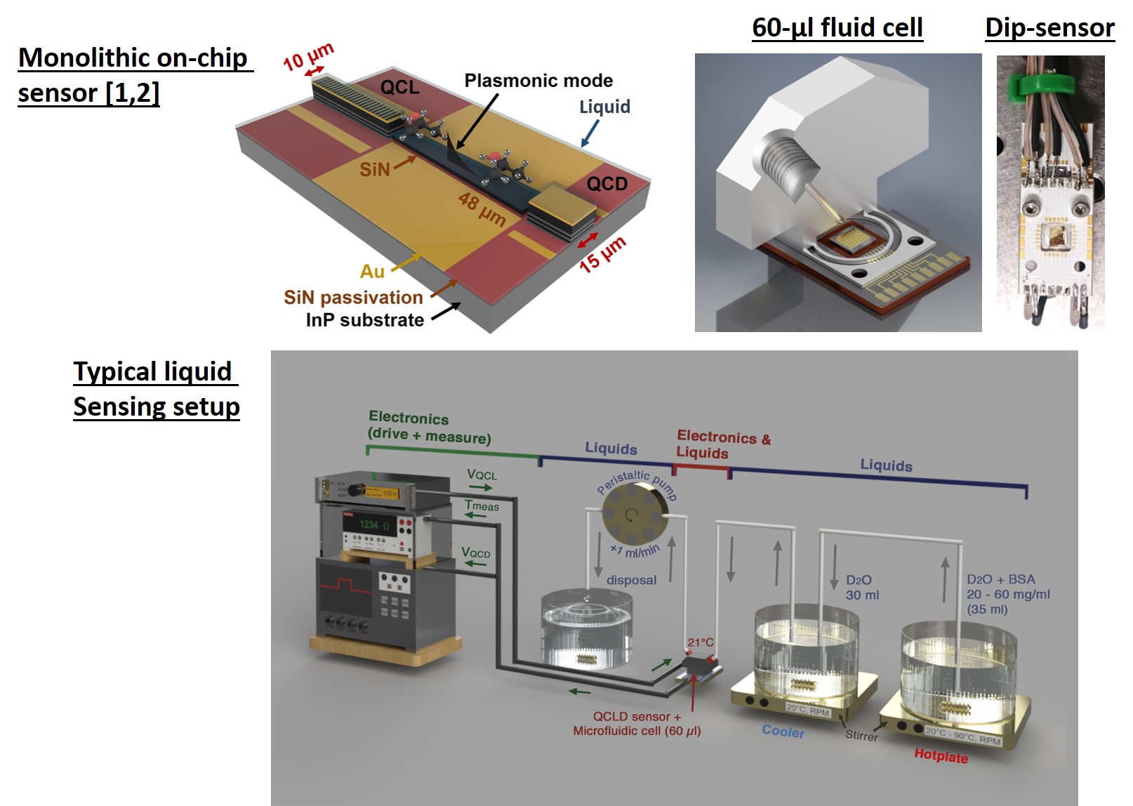
Combining QCL and QCD in a linear geometry with a connecting dielectric-loaded surface plasmon polariton waveguide to efficiently guide the mode emitted from the laser to the detector [1,2].
Such a geometry, enables the realization of liquid sensors for in situ monitoring of chemical reactions in real time. By either combining them with a custom-made fluid-cell hosting about 60 µl of volume or by directly submerging the whole chip into the liquid sample, allows to address different important settings in analytical chemistry [2].
b. Mid-infrared PICs for on-chip directing and chip-scale networks
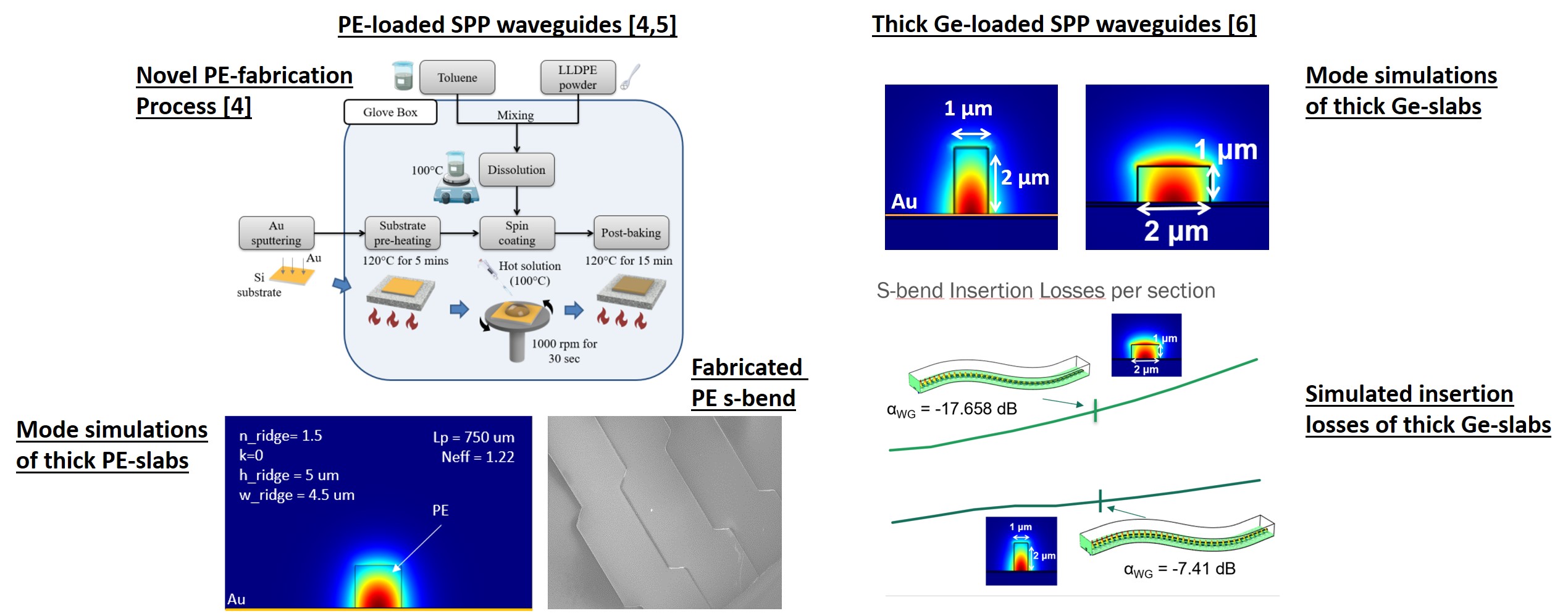
In a next level of PICs, more functionalities will be implemented into the device geometry. Besides on-chip amplifiers and modulators, this especially also means much more complex structures as realized in photonic integrated networks, know from the near-infrared spectral range. They allow to realize, e.g. on-chip interferometers like in Mach-Zehnder interferometers. For this the above introduced DLSPPs are not suitable, since the significant overlap of the plasmonic mode with the surrounding medium prevents to steer and direct the mode along bends on the chip-scale. For this we develop and have demonstrated different concepts like polyethylene-based DLSPPs [4,5] or using semiconductor-loaded SPPs (SLSPPs) with micrometer-thick Ge-slabs as topside confinement layer [6].
[1] B. Schwarz, P. Reininger, D. Ristanic, H. Detz, A. M. Andrews, W. Schrenk, and G. Strasser, Nat. Commun. 5, 4085 (2014).
[2] B. Hinkov, F. Pilat, L. Lux, P. L. Souza, M. David, A. Schwaighofer, D. Ristanic, B. Schwarz, H. Detz, A. M. Andrews, B. Lendl, and G. Strasser, Nat. Commun. 13, 4753 (2022).
[3] M. David, A. Dabrowska, M. Sistani, I. C. Doganlar, E. Hinkelmann, H. Detz, W. M. Weber, B. Lendl, G. Strasser, and B. Hinkov, Opt. Express 29(26), 43567 (2021).
[4] M. David, D. Disnan, A. Lardschneider, D. Wacht, H. T. Hoang, H. Detz, B. Lendl, U. Schmid, G. Strasser, and B. Hinkov, Opt. Mater. Express 12(6), 2168 (2022).
[5] M. David, A. Lardschneider, D. Disnan, H. T. Hoang, H. Detz, U. Schmid, G. Strasser, and B. Hinkov, in preparation.
[6] M. David, G. Marschick, E. Arigliani, N. Opacak, B. Schwarz, G. Strasser, and B. Hinkov, 48th European Conference on Optical Communication (ECOC), Basel, Switzerland, 18 – 22 Sept, 2022.