Passive optoelectronic devices
Research on Passive Optoelectronic Devices
Passive optoelectronic devices that are being used in our work mainly include various types of (passive) waveguides. They are semiconductor-based structures that can couple and guide optical modes. We use dielectric and plasmonic waveguides designed for mid-infrared wavelengths and combine them with suitable active devices such as quantum cascade lasers (QCLs), quantum cascade detectors (QCDs) and interband cascade lasers (ICLs). This allows us to use them in different types of applications including the spectroscopy of molecules in the liquid- and gas-phase, mode guiding and directing on the chip-scale for photonic integrated circuits (PICs) and networks as well as optical free-space telecommunication.
1. Waveguide structures for QCLs, QCDs and ICLs
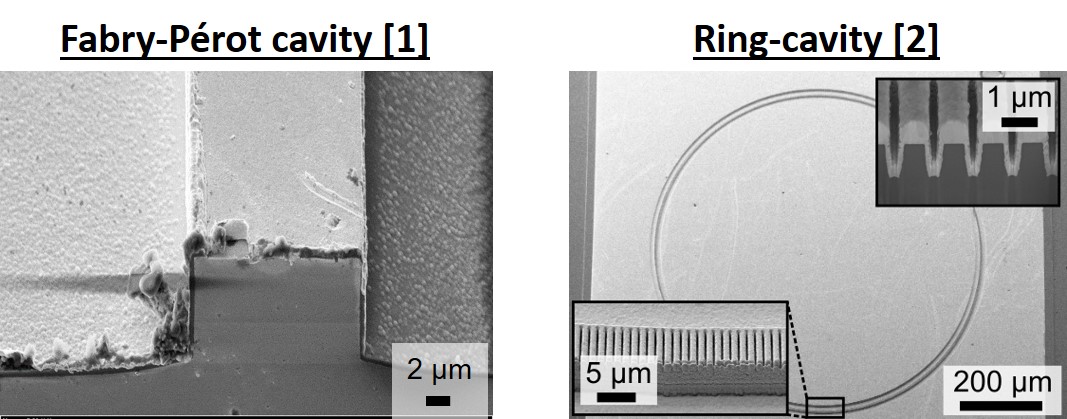
Typical waveguide structures that are used for (active) semiconductor devices, are based on dielectric cavities. They allow mode confinement on suitable mid-infrared scales together with low losses (<< dB/mm scale) that e.g. allow lasing emission from a QCL or ICL. They can be realized in different shapes including linear slab-waveguides [1] or ring-cavities [2], as shown by the following scanning electron microscope (SEM) images:
a. Mode control in dielectric cavities
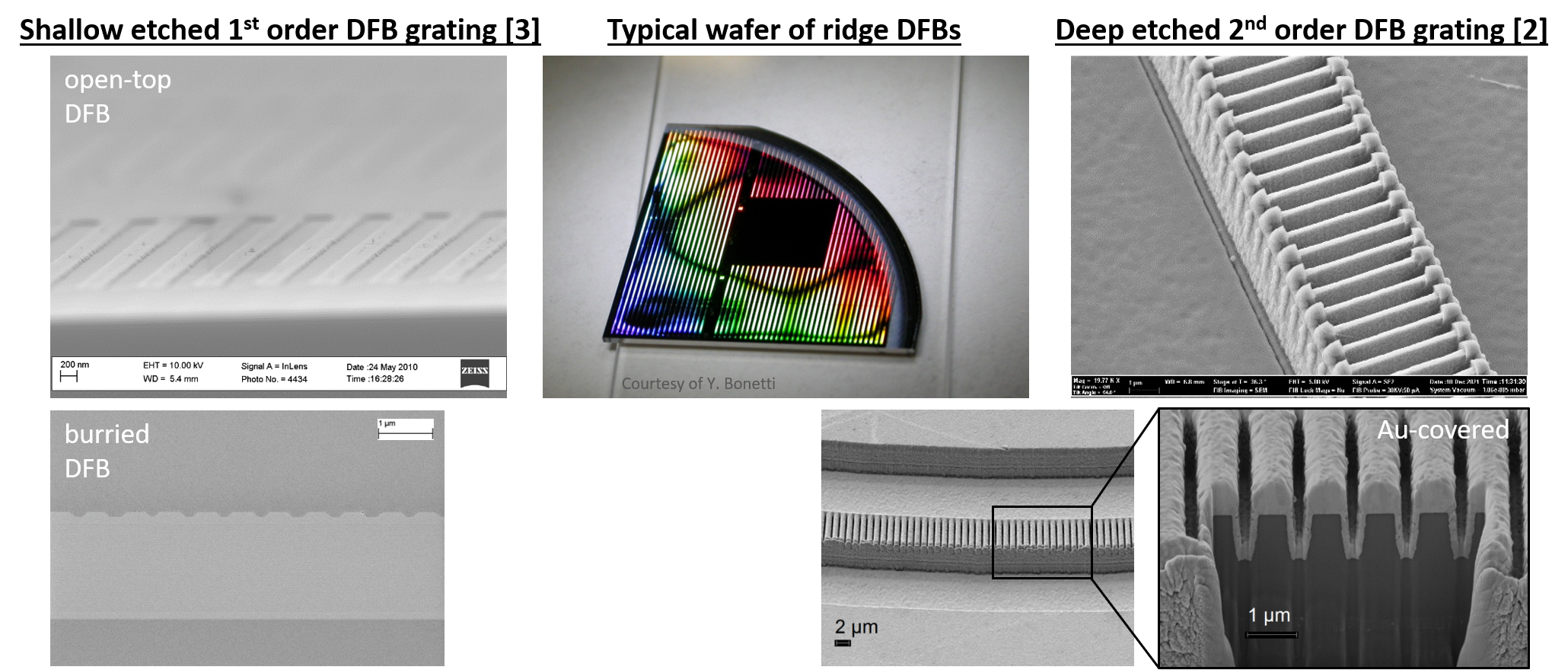
Linear (slab-)waveguides lead to multimode-support of such dielectric cavities (cp. Fabry-Pérot waveguides). Consequently, additional measures have to taken to control the modal emission of optoelectronic devices. This includes the implementation of distributed feedback (DFB) gratings, i.e. periodic modulations of the refractive index (real or imaginary part or both). Besides tailoring the spectral emission, DFB gratings also enable realizing vertical emitting/detecting configurations as demonstrate e.g. in [2].
In the following a few examples of such grating structures, implemented into QCL-ridge and ICL-ring cavities are shown:
2. Novel plasmonic waveguides for the mid-infrared
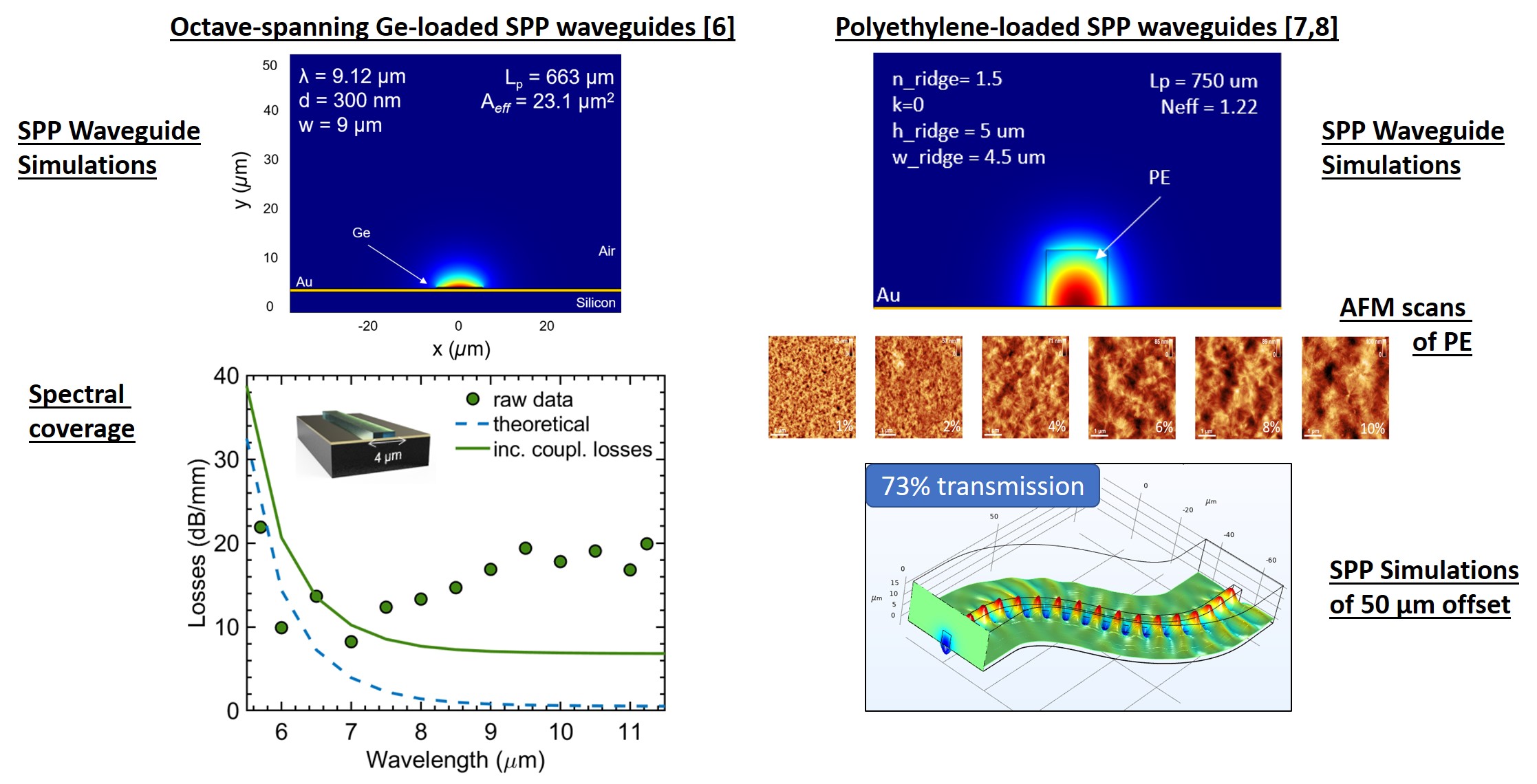
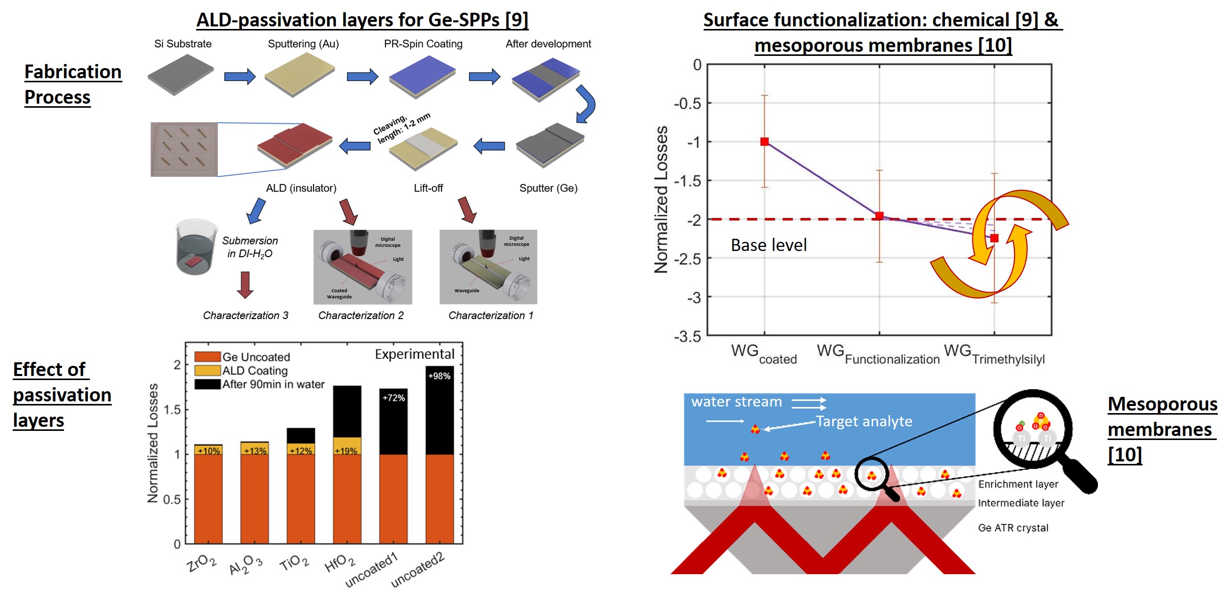
Another important and rather novel type of waveguides is based mid-infrared plasmonics, i.e. the collective electron oscilations at an interface between two materials with sign change of the dielectric function (e.g. a metal-dielectric interface). While plasmonics at visible and near-IR frequencies is an established field, benefitting its close proximity to the plasma-frequency of various metals, the situation is more difficult in the mid-infrared. Well-known concepts from shorter wavelength like metal sheets exposed to air with their sub-wavelength mode confinement, lead to propagating mid-infrared surface plasmon polariton (SPP) modes with poor vertical confinement. The mode typically extends 10 times or more of its wavelength into the surrounding medium [4]. Fortunately, this issue can be solved, by applying the concept of dielectric-loading. By implementing a suitable dielectric layer with high permittivity in the form of a slab on top of the metal layer, vertically confines the mode on the order of its wavelength to the surface, while enabling propagation lengths on the order of 100s of micrometer or even millimeters [5]. We picked up this concept and developed it further towards broadband mid-infrared coverage [6], on-chip plasmonic mode guiding and directing [7,8], surface passivation and functionalization for the sensitive and selective spectroscopy of liquids [9,10] and in general realizing chip-scale PICs and photonic networks that can find their application in the optical free-space communication [11]:
[1] G. Marschick, M. David, E. Arigliani, N. Opacak, B. Schwarz, M. Giparakis, A. Delga, M. Lagree, T. Poletti, V. Trinité, A. Evirgen, B. Gerard, G. Ramer, R. Maulini, J. Butet, S. Blaser, A. M. Andrews, G. Strasser, and B. Hinkov,
Opt. Express 30(22), 40188-40195 (2022).
[2] H. Knötig, B. Hinkov, R. Weih, S. Höfling, J. Koeth, and G. Strasser, Appl. Phys. Lett. 116, 131101 (2020).
[3] B. Hinkov, A. Bismuto, Y. Bonetti, M. Beck, S. Blaser, and J. Faist, Electron. Lett. 48(11), (2012).
[4] S. Law, V. Podolskiy, and D. Wasserman, Nanophotonics 2(2), 103-130 (2013).
[5] B. Schwarz, P. Reininger, D. Ristanic, H. Detz, A. M. Andrews, W. Schrenk, and G. Strasser, Nat. Commun. 5, 4085 (2014).
[6] M. David, A. Dabrowska, M. Sistani, I. C. Doganlar, E. Hinkelmann, H. Detz, W. M. Weber, B. Lendl, G. Strasser, and B. Hinkov, Opt. Express 29(26), 43567 (2021).
[7] M. David, D. Disnan, A. Lardschneider, D. Wacht, H. T. Hoang, H. Detz, B. Lendl, U. Schmid, G. Strasser, and B. Hinkov, Opt. Mater. Express 12(6), 2168 (2022).
[8] M. David, A. Lardschneider, D. Disnan, H. T. Hoang, H. Detz, U. Schmid, G. Strasser, and B. Hinkov, in preparation.
[9] M. David, I. C. Doganlar, D. Nazzari, E. Arigliani, D. Wacht, M. Sistani, H. Detz, G. Maisons, G. Ramer, B. Lendl, W. M. Weber, G. Strasser, and B. Hinkov, in preparation.
[10] D. Wacht, M. David, B. Hinkov, H. Detz, A. Schwaighofer, B. Baumgartner, and B. Lendl, Appl. Spectrosc. 76(1), 141 (2021).
[11] M. David, G. Marschick, E. Arigliani, N. Opacak, B. Schwarz, G. Strasser, and B. Hinkov, 48th European Conference on Optical Communication (ECOC), Basel, Switzerland, 18 – 22 Sept, 2022.