Novel Optoelectronic Materials
Research on Novel Optoelectronic Materials
An important part in the field of developing the next generation of mid-infrared optoelectronic devices is dedicated to novel materials and materials systems [1-3]. This is especially true for devices aiming at the THz spectral range. So far this part of the electromagnetic spectrum still remains in a premature state, where e.g. quantum cascade lasers (QCLs) are still limited to temperatures significantly below room temperature. Even though very advanced III-V semiconductor material systems like GaAs and InP were used, the performance advancements did continuously slow down after the first demonstration of a THz-QCL in 2002 [4]. They were indeed long bound to cryogenic temperatures below 200K [5] and just recently new milestones could be achieved by demonstrating thermoelectrically cooled GaAs-THz-QCLs at operation temperatures of 210K ([6], 2019) and 250K ([7], 2021).
However, novel disruptive approaches are still of interest to e.g. finally achieve THz-QCL emission at room temperature or develop other novel optoelectronic devices for the mid-infrared and THz spectral range.
One such approach is based on ZnO, a novel material systems for mid-IR and THz-optoelectronics. Its advantage is a twice as high LO-phonon energy (72 meV) as compared to the GaAs material system (36 meV). This is beneficial in two ways. First of all, it pushes the energy of the non-radiative LO-phonon transitions, which are competing with the optical transition, further away from the thermal energy at room-temperature. It is therefore predicted, that ZnO-devices show higher operational temperatures together with better performance close to room-temperature and above [8]. Second, it unlocks a new spectral range for device emission, that was previoulsy not reachable due to the Restrahlenband of GaAs [3].
In order to realize ZnO QC based devices, a novel suitable device fabrication routine had to be developed for structuring tailored low-cavity-loss devices [1]. Based on it, we realized two types of quantum cascade devices in the non-polar m-plane orientation of ZnO, to avoid internal fields, within the EU project “ZOTERAC”. The devices are exploiting ZnO quantum wells with ZnMgO barriers. One is the first ZnO-based mid-IR QCD at a wavelength of ZZ µm [2] and the other constitutes the demonstration of the first THz electroluminescence in the ZnO-based material system. Those two examples are a clear indication of the significant progress that we could achieve in designing and controlling the ZnO material system.
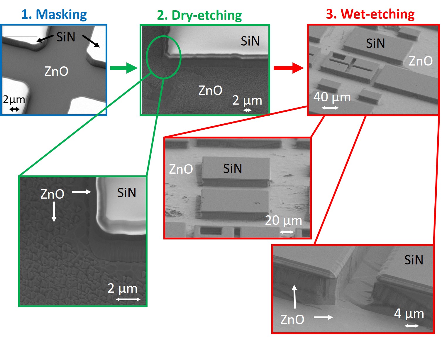
a. Developing a Processing Routine for m-plane ZnO/ZnMgO Optoelectronic Devices [1]
ZnO is a new material to intersubband optoelectronics and thus its processing and patterning into suitable waveguide structures characterized by low optical and electrical losses was the first challenge. We developed a new fabrication scheme, built around a dry etching ICP-RIE process in a CH4-chemistry with SiN hardmask. A following short dip in diluted HCl helps to clean-up the surface and remove defects and roughness from the previous dry etching. In the end, the devices are submerged in H2O2 for electrical passivation of the sample surface and avoiding electrical surface leakage currents which are otherwise present. The important steps are displayed in the following. More details can be found in the following publication: [1]
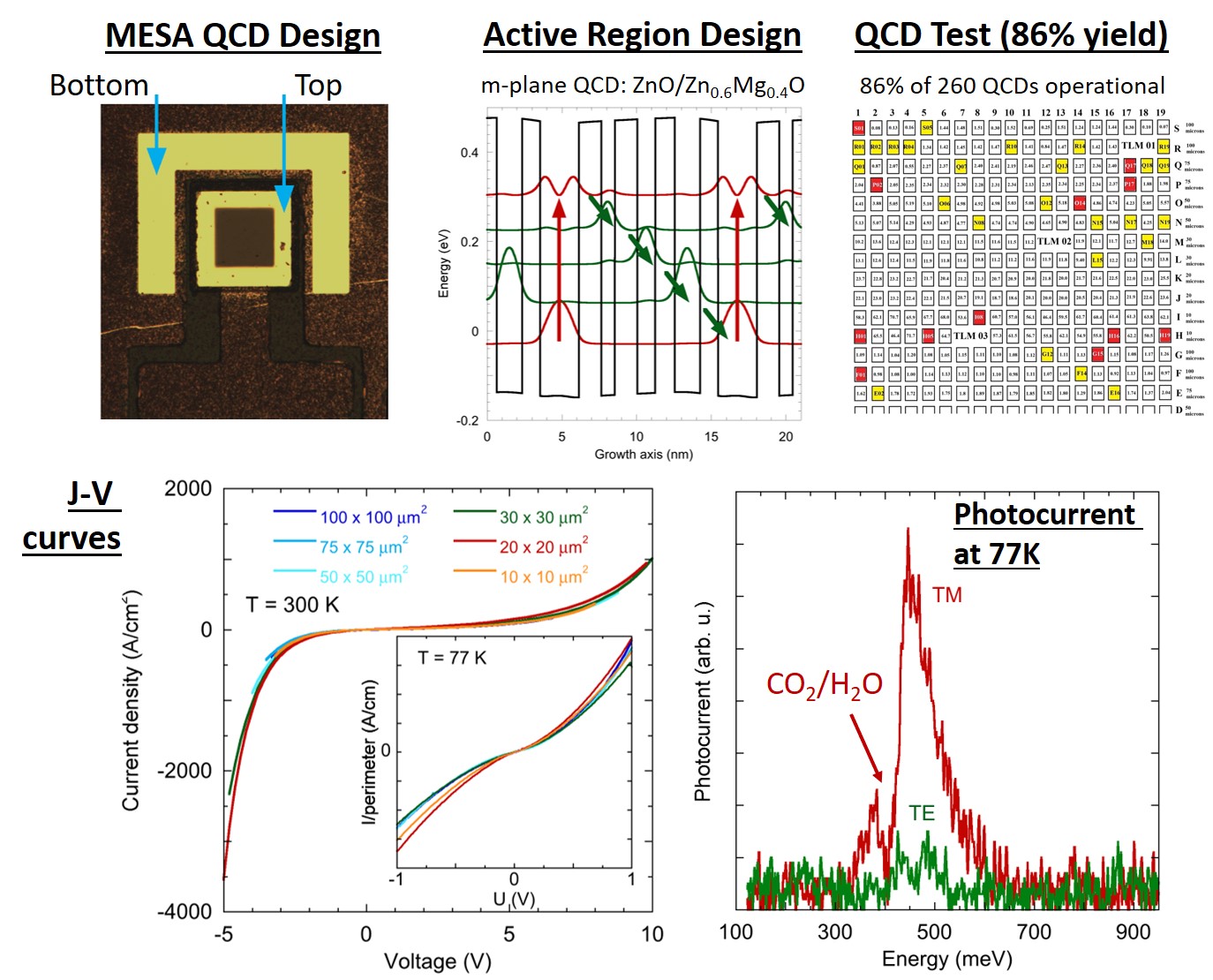
b. Mid-infrared QCDs based on m-plane ZnO/ZnMgO [2]
For demonstrating the capability to realize QC devices in the ZnO material system, we chose QCDs in the first step. Their operation has a lower demand on the quality of the fabrication and the resulting (optical) losses, as e.g. for the QCL. Therefore, QCDs are a good first example for an initial demonstration of our processing capabilities of m-plane ZnO. We designed and realized mid-IR QCD MESA structures with an opening in the topside metallization for incoupling the light. With this we show a peak absorption at a wavelength of 3 µm, together with a very high fabrication yield of 86% of operational devices from in total 260 tested QCDs, and a peak responsivity of 0.15 mA/W at 77K for a Brewster-angle illumination measurement.
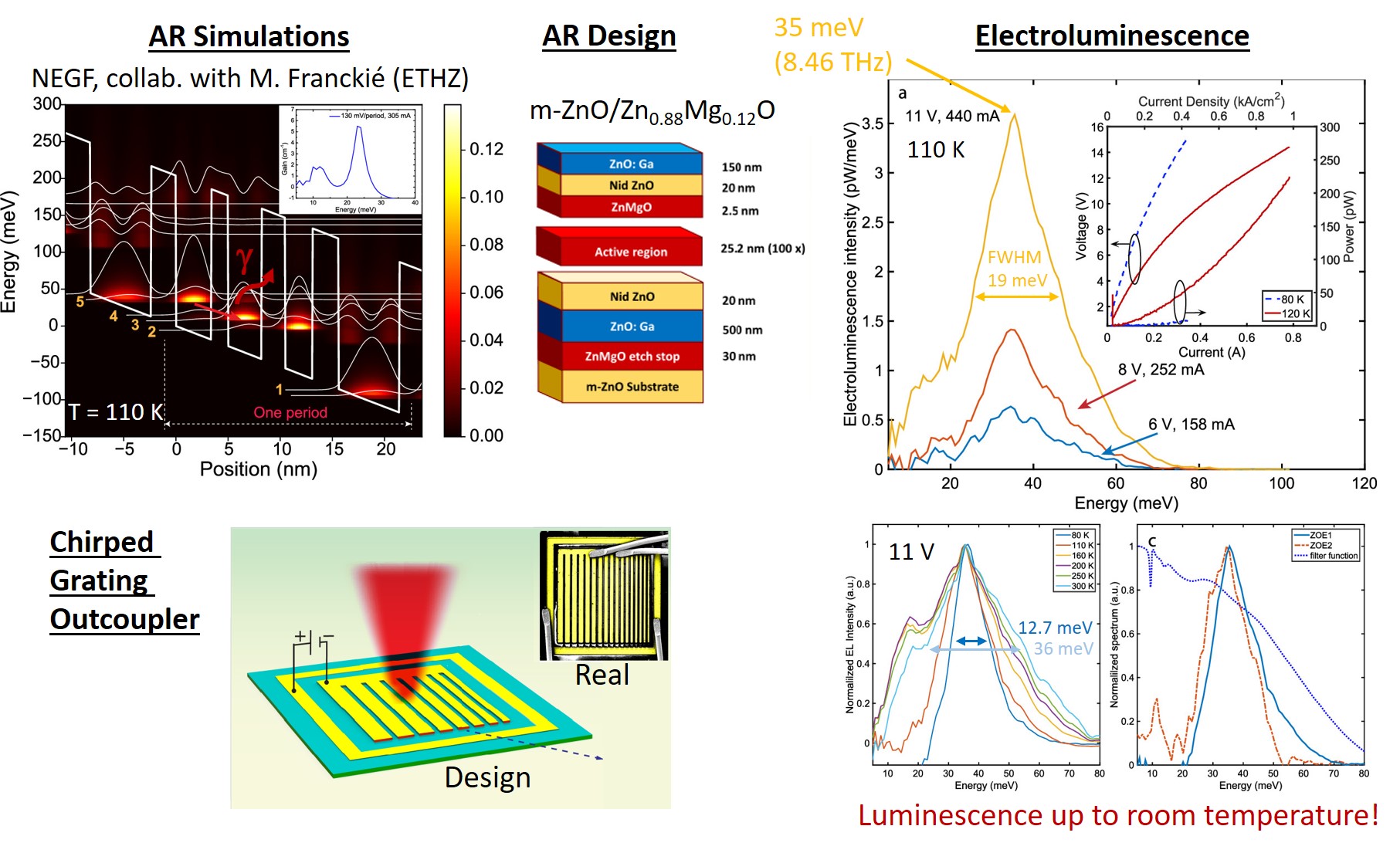
c. Towards ZnO-based THz-QCLs: the 1st THz-Eletcroluminescence from ZnO QC Structures [3]
After showing tailored detector operation in the previous section, we will show the realization of a THz emitter in the ZnO material system. Again, square MESAs were fabricated, but this time with a chirped 2nd-order topside DFB grating. The 2nd order leads to vertical light coupling, while the chirp in the grating enables to address a wide range of frequencies. This is beneficial, since designing and suitably realizing the device is much more challenging in a novel material system such as ZnO as compared to e.g. GaAs. And indeed, the first intersubband electroluminescence from a ZnO/ZnMgO-based heterostructure could be demonstrated with this approach. It peaks at around 8.5 THz and the luminescence signal remains measurable up to room temperature.
[1] B. Hinkov, H. T. Hoang, M. Hugues, J.-M. Chauveau, and G. Strasser, Semicond. Sci. Technol. 36, 035023 (2021).
[2] A. Jollivet, B. Hinkov, S. Pirotta, H. Hoang, S. Derelle, J. Jaeck, M. Tchernycheva, R. Colombelli, A. Bousseksou, M. Hugues, N. Le Biavan, J. Tamayo-Arriola, M. Montes Bajo, L. Rigutti, A. Hierro, G. Strasser, J.-M. Chauveau, and
F. M. Julien, Appl. Phys. Lett. 113, 251104 (2018).
[3] B. Meng, B. Hinkov, N. Le Biavan, H. T. Hoang, D. Lefebvre, M. Hugues, D. Stark, M. Franckié, A. Torres-Pardo, J. Tamayo-Arriola, M. M. Bajo, A. Hierro, G. Strasser, J. Faist, and J.-M. Chauveau, ACS Photon. 8, 343 (2021).
[4] R. Köhler, A. Tredicucci, F. Beltram, H. E. Beere, E. H. Linfield, A. G. Davies, D. A. Ritchie, R. C. Iotti, and F. Rossi, Nature 417, 156 (2002).
[5] S. Fathololoumi, E. Dupont, C. W. I. Chan, Z. R. Wasilewski, S. R. Laframboise, D. Ban, A. Mátyás, C. Jirauschek, Q. Hu, and H. C. Liu, Opt. Express 20(4), 3866 (2012).
[6] L. Bosco, M. Franckié, G. Scalari, M. Beck, A. Wacker, and J. Faist, Appl. Phys. Lett. 115, 010601 (2019).
[7] A. Khalatpour, A. K. Paulsen, C. Deimert, Z. R. Wasilewski, and Q. Hu, Nat. Photon. 15, 16-20 (2021).
[8] E. Bellotti, K. Driscoll, T. D. Moustakas, and R. Paiella, J. Appl. Phys. 105, 113103 (2009).